Machine Learning and Deep Learning
ML and DL for heat transfer design
|
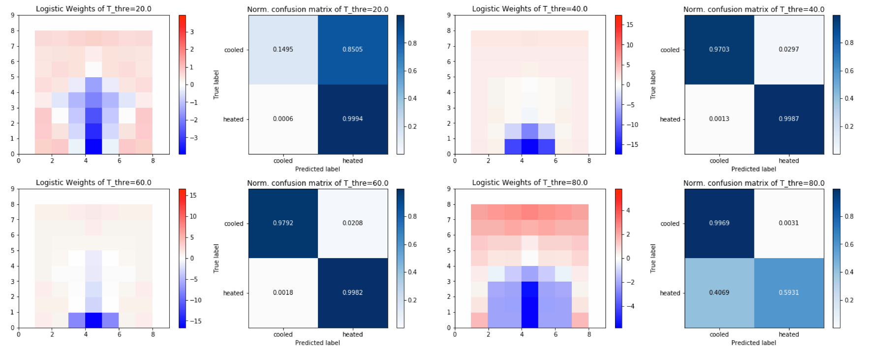
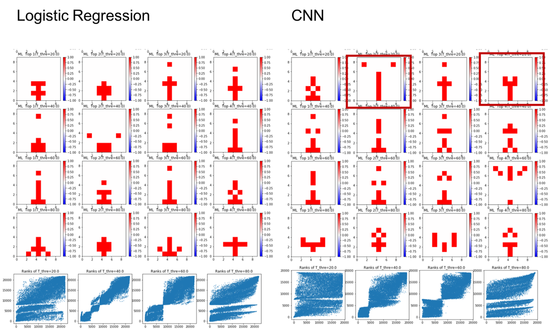
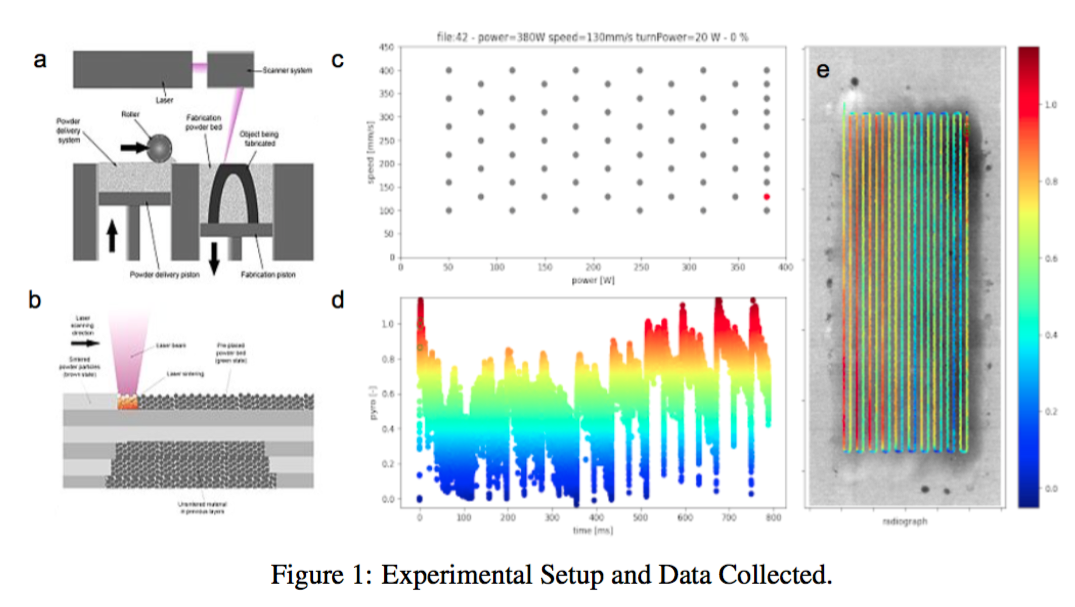
Video+CNN for additive manufacturing
Machine learning for additive manufacturing
| ||
Optics, Nanophotonics and Nanofabrication
Transient Reflective Probing |
Nano fabrication
|
|
Laser sources: CW, nanosecond lasers
Optics: PBS, 1/4 wave, 1/2 wave, notch filter Oscilloscope, photodetector, color camera Motion control, NC programming. 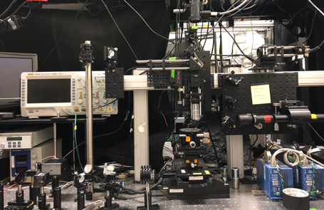
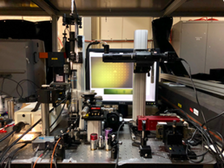
Home-built MicroscopeMicroscale transmission and reflection probing with different light sources.
|
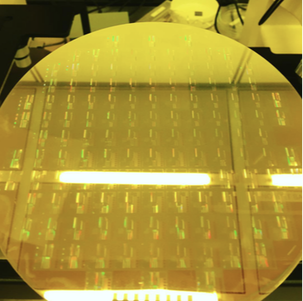
* Nanofabrication for Non-MOS wafer scale photonics metasurfaces and electrical test circuits:
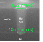
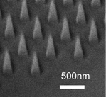
-250nm node layout design (L-edit, Tanner) -Photolithography(ASML 5500/300) -RIE(Lam Research, STS) -Deposition(Ebeam Evaporation, ALD, LPCVD, PECVD) -Metrology(AFM, Ellipsometry, SEM, Nanospec, FIB) -Epitaxial growth of Ge on Si (Applied Materials, Centura) -CD reduction: double deposition and over-etch *Tool development: Upgrade the Laser-assisted chemical vapor deposition (LACVD) tool with -additional high power nanosecond pulsed laser. Carried out damage threshold, beam alignment and focusing tests. -additional vacuum chamber *Research and Process Development: -Laser-assisted atomic layer etching of amorphous silicon film and silicon wafers with Cl2 gases.
|
Disclaimer: The schematics and images are originally created by Letian Wang. Most of them are not published. (c) Letianwang.me 2018
Hardware Development
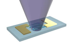
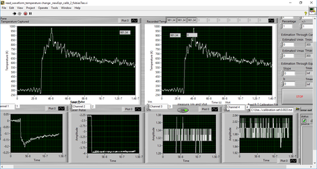
Micro thermometer with RF electrical measurement and LabView interface |
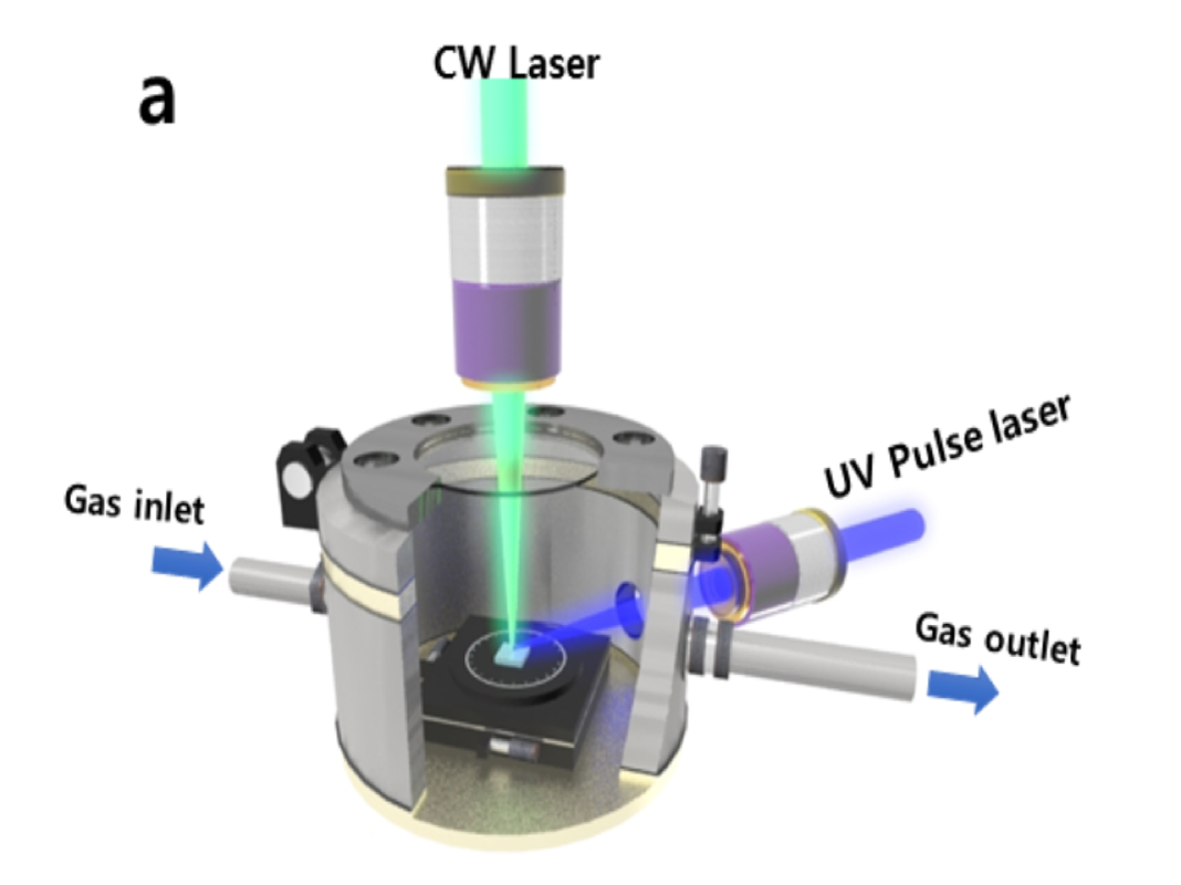
Multi-beam Laser Chemical Processing |
|
|
Simulation
Simulator for heat transfer and phase change (home-built for LTL, collaborated with Jung Bin In)
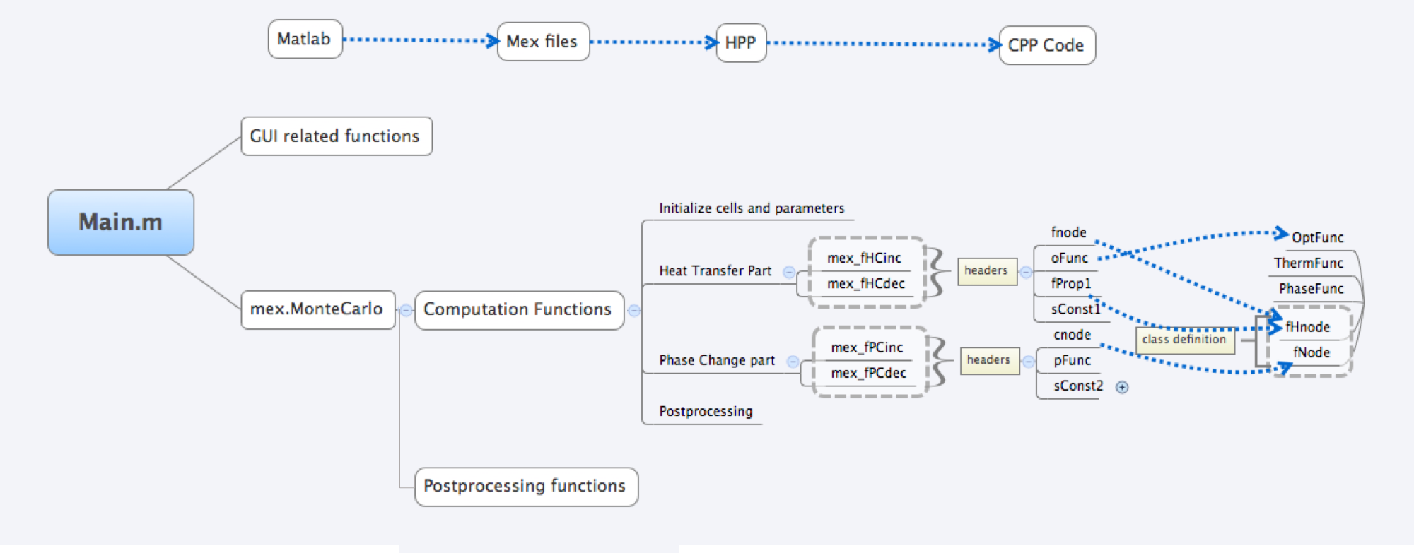
Numerical Scheme(ADE)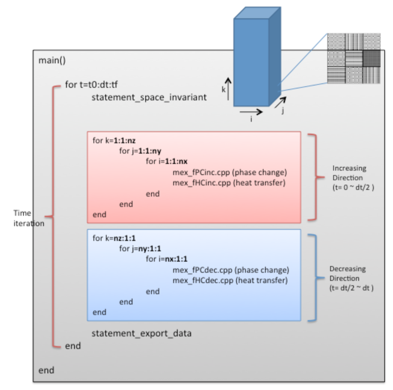
|
GUI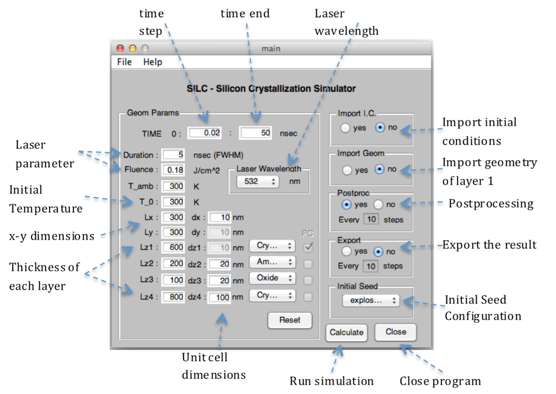
|
Progress Monitor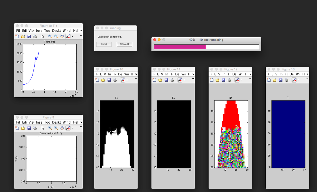
|
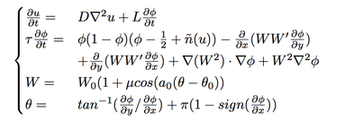
Crystallization based on Phase Field Function (CS 294: Software Engineering for Scientific Computing)
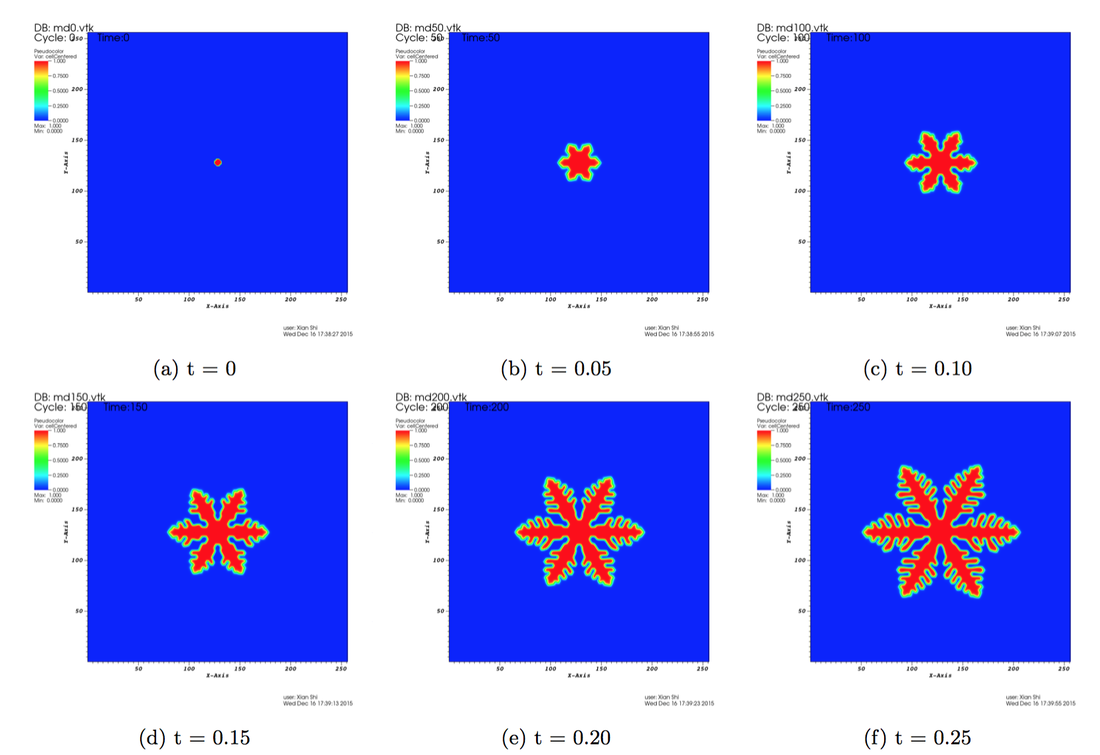
|
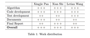
I was in charge of the initiation of the idea, basic algorithm search and test development. Please check my Github and Report.
| ||||
Commercial Simulator
Lumerical FDTDMie-scattering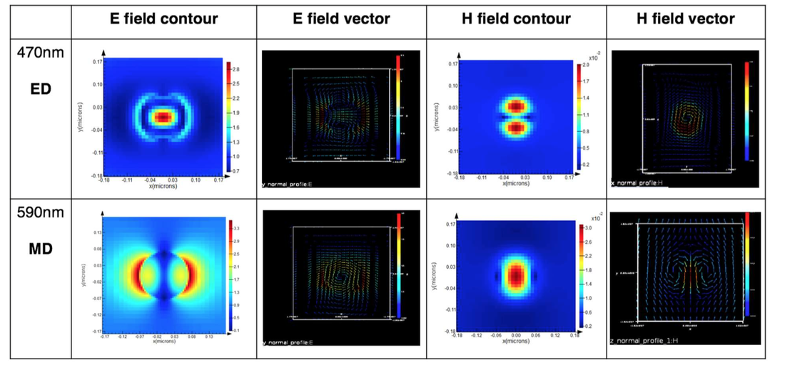
Pancharatnam-Berry Phase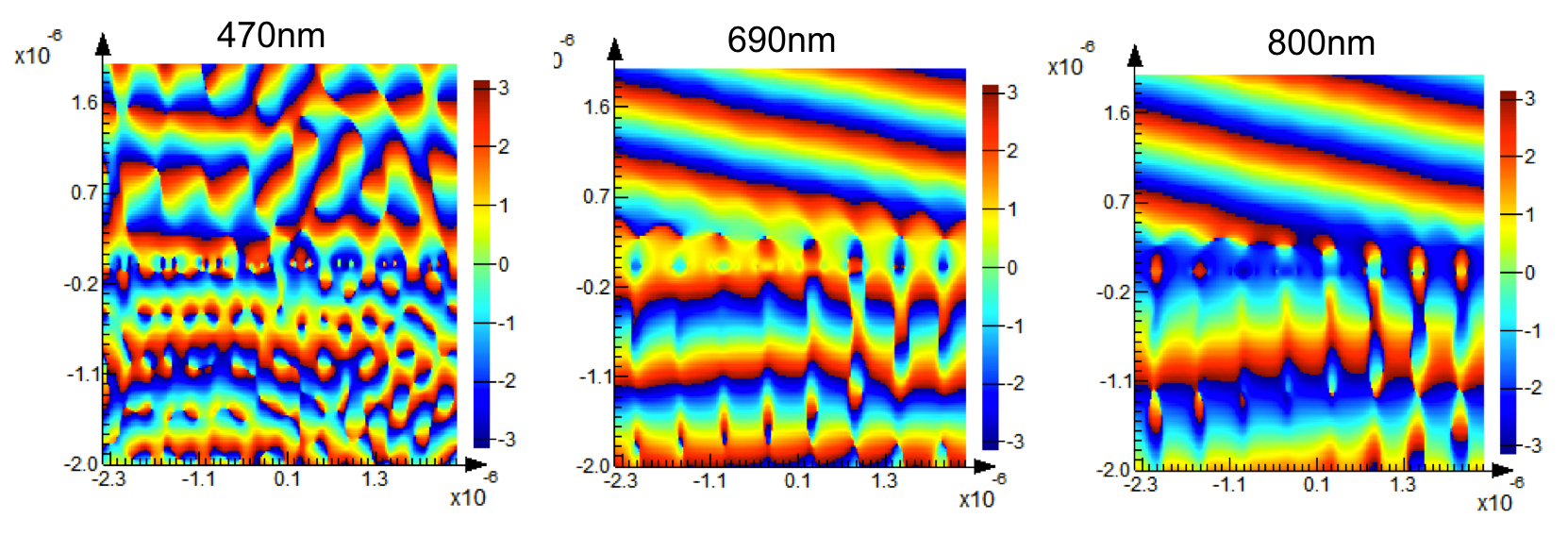
|
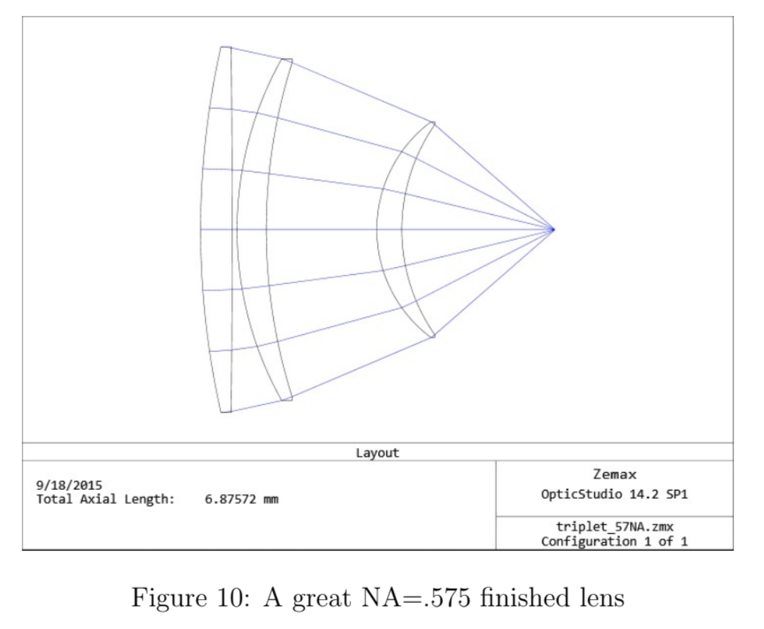
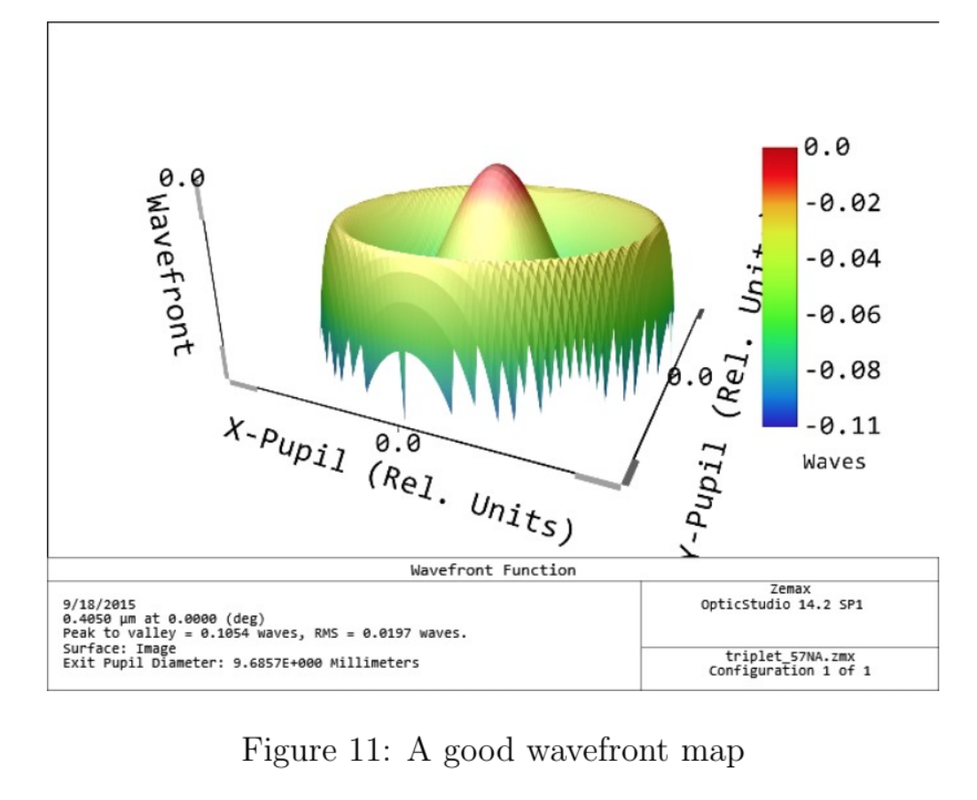
Zemax (EE 218A, Laura Waller)
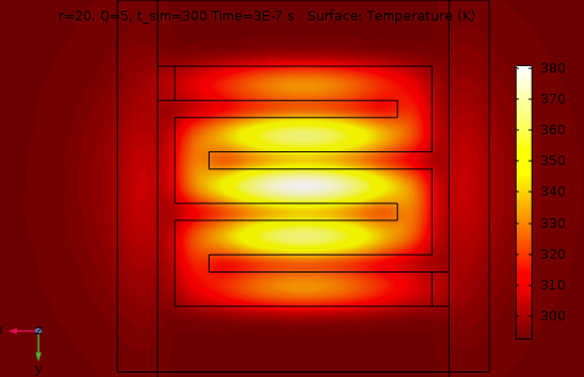
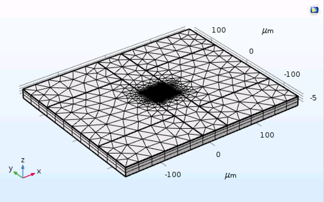
COMSOL(thermal, fluid, electrical)
LTspice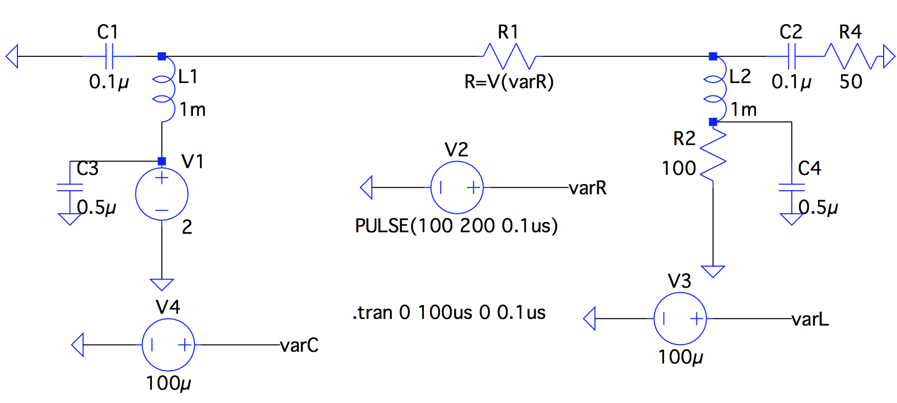
|